 EN
EN
 RU
RUWhy “How Thick?” Is the First Question You Should Ask
Walk through any electronics market in Shenzhen, Frankfurt, or Silicon Valley and you will see booth after booth promising “quick-turn PCBs.” Yet the single biggest source of re-quotes, delayed shipments, and field failures is not line-width or via-size—it is thickness. Pick the wrong value and your board may not fit the enclosure; impedance goes out of spec; connectors refuse to seat; customs officers question the declared weight; and, worst of all, the product fails once it is in the customer’s hands. In short, thickness is where mechanical engineering, electrical performance, logistics, and cost control intersect. Get it right and the rest of the project flows. Get it wrong and every downstream department will blame “the PCB guy.” This article gives you the insider view—straight from a trade-desk veteran—so you can speak the language of your fabricator, your quality team, and your CFO in the same sentence.
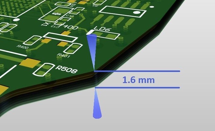
The One Number You Can Recite in Your Sleep: 1.57 mm
If you remember nothing else, remember 1.57 mm (0.062 in). Eighty percent of the 100 billion cm² of rigid board area produced annually is still ordered at, or very close to, this nominal value . The reason is historical: early punch-card and tape-automated drills were spaced for 1/16-inch laminate, so component vendors tooled their connectors for that height. When CAD and CNC took over, the tooling budget had already been amortized; nobody wanted to re-tool unless there was a compelling reason. Today the 1.57 mm thickness is baked into:
94 % of edge-card connectors (PCIe, DIMM, etc.)
90 % of sheet-metal enclosures and guide-rail slots
99 % of off-the-shelf solder pallets and test fixtures
Therefore, unless your industrial-design team has a crystal-clear justification, you start every quotation at 1.57 mm and let other requirements pull you away from it deliberately, not accidentally.
The Complete “Menu” of Standard Thicknesses
Fabricators stock laminate cores in discrete steps. Ask for anything between those steps and you pay a premium, sometimes 15 %–25 %, because the factory must combine thinner cores or custom-grind a laminate.
| Nominal (mm) | Inch | Typical Use-Cases |
|---|---|---|
| 0.40 | 0.016″ | SIM-cards, camera modules, sensor stickers |
| 0.60 | 0.024″ | Wireless earbuds, IoT tags |
| 0.80 | 0.031″ | Smartphones, SSDs, memory cards |
| 1.00 | 0.039″ | Tablets, portable instruments |
| 1.20 | 0.047″ | Automotive display controllers |
| 1.60 (1.57) | 0.062″ | Universal default |
| 2.00 | 0.079″ | Backplanes, thick copper LED boards |
| 2.40 | 0.094″ | Industrial drives, engine-control units |
| 3.20 | 0.126″ | Power inverters, railway electronics |
Rule of thumb: every 0.5 mm you add above 1.6 mm raises material cost by ~10 % and drilling cycle-time by ~8 % . Go below 0.8 mm and you need special transport trays to prevent board breakage—another hidden cost.
Tolerance: The Silent Profit Killer
Buyers often negotiate copper price by the gram yet forget that thickness tolerance can eat 7 %–10 % of your electrical budget at no benefit to you. IPC-6012 defines three performance classes :
Class 1 (consumer gadgets): ±10 %
Class 2 (industrial): ±8 %
Class 3 (medical/aerospace): ±5 %
On a 1.6 mm board, Class 1 therefore allows 1.44 mm–1.76 mm. If you design a 50 Ω microstrip on 0.2 mm prepreg, that ±10 % dielectric thickness can swing impedance ±5 Ω, enough to fail eye-mask in USB-C or PCIe-Gen4. The fix is to state both nominal thickness and tolerance class on your fabrication drawing, and—if you really need tighter control—pay the 5 % surcharge for “controlled thickness” instead of re-spinning 2,000 boards later.
Copper Weight Adds (Real) Millimeters
Copper is sold by weight: 1 oz/ft² = 35 µm per layer. But the finished foil is plated up in holes and on outer layers, so outer foils end up ~38 µm–45 µm. If your stack-up is:
4 layers, 1 oz inner, 1 oz outer
0.2 mm prepreg ×2, 0.6 mm core
The copper alone contributes ~0.14 mm, almost 9 % of the final 1.6 mm. When you jump to 2 oz (70 µm) or 3 oz (105 µm) to carry high current, you can easily overshoot your mechanical envelope unless you compensate by thinning the core. Experienced trade-desk engineers therefore quote “copper-adjusted thickness” and warn customers if the finished board will exceed 1.7 mm on a 1.6 mm nominal order .
Multilayer Magic: Why 8 Layers Can Still Be 1.6 mm
Newcomers assume that more layers automatically mean a thicker board. In reality, an 8-layer HDI mobile board can be 0.8 mm, whereas a 2-layer coinverter for a solar inverter can be 3.2 mm. The trick is core/prepreg selection. Standard FR-4 cores start at 0.05 mm and run upward in 0.1 mm increments; prepregs go as thin as 0.04 mm (106 type). By mixing ultra-thin prepregs with 0.1 mm cores, you can pack twelve conductive layers inside 1.6 mm and still meet drill aspect-ratio rules (≤10:1 for mechanical vias). The trade-off is cost: ultra-thin laminates are 30 %–50 % more expensive and require laser-drilling for micro-vias, but they preserve the golden 1.6 mm outer envelope that your mechanical team already tooled for.
Thermal & Mechanical Reality Check
Thickness is a free heatsink. Doubling board thickness from 1.6 mm to 3.2 mm can cut thermal resistance through the board by ~35 %, letting your MOSFETs run 8 °C cooler—often worth an entire dollar of aluminum extrusion you no longer need . Conversely, in handheld devices every 0.1 mm you shave off the PCB translates into 0.1 mm more battery volume, which could mean 50 mAh extra capacity. Marketing departments love that story, so they push for 0.6 mm boards. The supply-chain catch is that 0.6 mm boards require 0.13 mm connectors, which cost 2× the standard 1.6 mm versions and have 30 % lower current rating. Your BoM savings evaporate while reliability suffers. The takeaway: treat thickness as a system-level specification, not a PCB-level afterthought.
Cost Playbook: How to Save 12 % Without Sacrificing Performance
- Default to 1.6 mm unless ID or thermal analysis forbids it.
- Specify IPC Class 2 tolerance; upgrade to Class 3 only when mandatory.
- Use 1 oz outer / 0.5 oz inner copper for signals; jump to 2 oz only on dedicated power layers, not everywhere.
- If you need 2 oz on outer layers, drop the core 0.1 mm to stay ≤1.7 mm finished—avoiding a custom-thickness surcharge.
- Consolidate all unique thicknesses into one panel; mixing 0.8 mm and 1.6 mm on the same 18 × 24 in panel incurs a 5 % penalty for “split thickness” handling.
- Book 10 % excess copper area on inner layers; it balances layer thickness and improves lamination yield, indirectly holding thickness tolerance.
Checklist You Can Paste into Your Next RFQ
□ Tolerance class: IPC-6012 Class ___ (1/2/3)
□ Copper weight each side: ____ oz (0.5/1/2/3)
□ Finished thickness including plating: max ____ mm
□ Bow & twist: ≤0.75 % (IPC-6012) or custom ___ %
□ Number of layers: ___ (same thickness OK)
□ Impedance control: ___ Ω ±___ % (if applicable)
□ Special materials: FR-4 / Rogers / Aluminum / ___
□ Surface finish: HASL / ENIG / Imm-Sn / Imm-Ag / ___
□ Panel utilization: single thickness / mixed OK? ___
Future-Proofing: 0.2 mm and 4 mm Are Coming
Foldable phones are driving 0.2 mm polyimide rigidizers, while 800 V EV chargers are pushing 4 mm aluminum-core boards. Both extremes are still niche, but NPI (new-product-introduction) teams must already budget for them. Start qualifying suppliers now; by 2028 these odd thicknesses will be as routine as 0.8 mm is today. The early bird gets both the yield learning curve and the negotiating leverage.
Key Takeaways for Busy Managers
- 1.57 mm is the golden thickness—deviate on purpose, not by accident.
- Thickness tolerance is a hidden cost; specify IPC class explicitly.
- Copper weight adds real millimeters—account for it in your mechanical stack-up.
- Multilayer count ≠ thickness; ultra-thin laminates let you stay at 1.6 mm.
- Treat thickness as a thermal and BoM lever, not just a mechanical datum.
- Lock the six-point checklist into your ERP template and watch re-quote rates drop 30 %.