 EN
EN
 RU
RUSMT Printed Circuit Board Assembly
ISO | UL | IATF16949| RoHS | Automated SMT production | SMT prototype PCBs in small / large quantities
Request A Free Quote
What is SMT assembly?
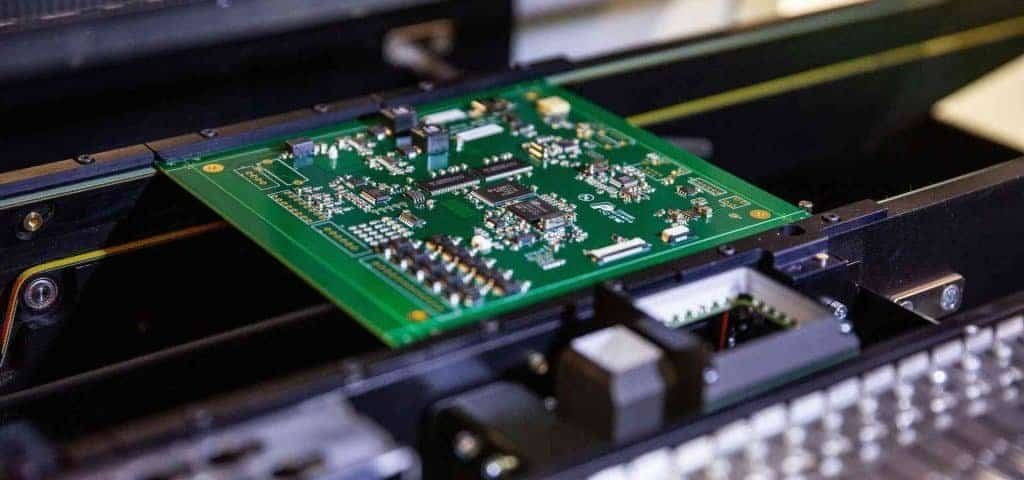
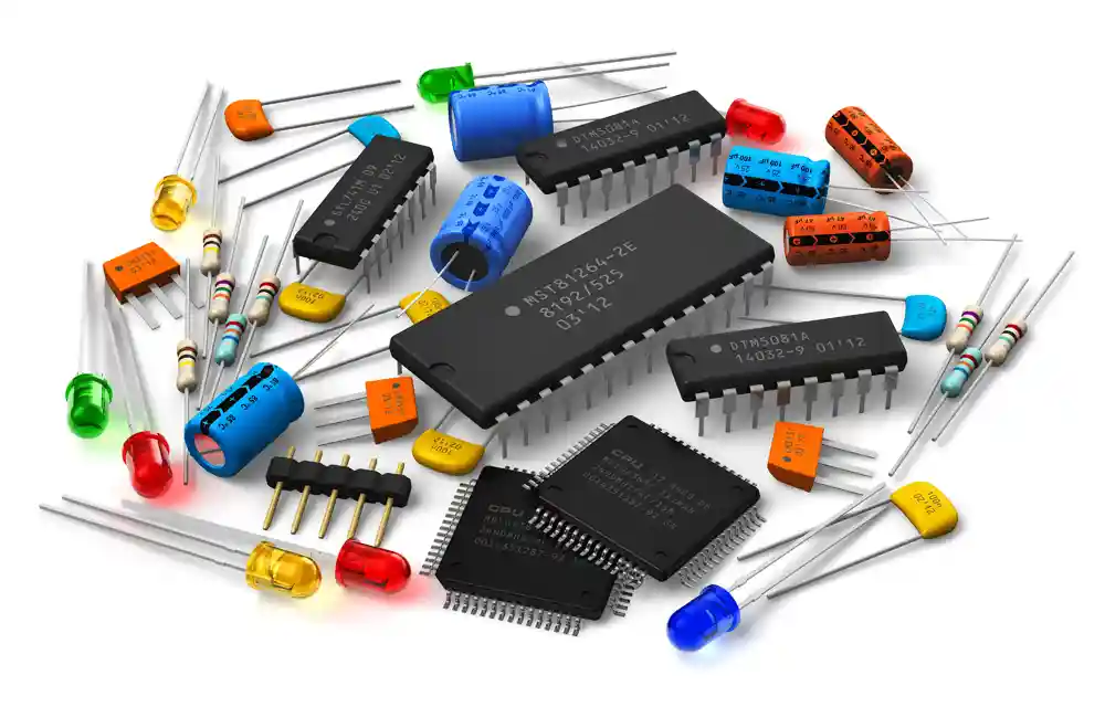
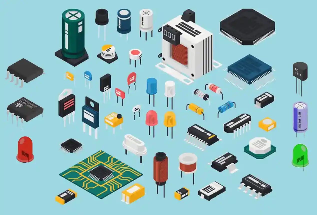
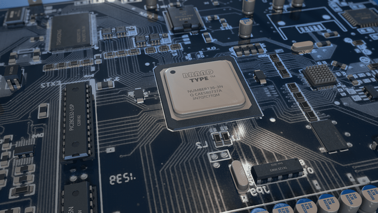
Surface mount technology or SMT is the most widely used method of assembling electronic modules, which reduces cost and ensures the high quality of the final product. Surface mount technology or SMT is a method for producing electrical circuits in which the components are mounted or placed directly onto the surface of printed circuit boards or PCBs and the electrical device that is soldered to the PCB is called a surface mount device or an SMD for sure by employing SMT the production process speeds up, but a risk of defects also increases due to the component miniaturization and to the denser packing of boards. A Zener diode and some capacitors are shown below in SMD package.
In this page, we will write some manufacturing steps of the automatic SMT process as well as the additional control steps and the automated selective soldering of through-hole components.
What Are The advantages of Surface mount technology?
There are many advantages of the SMT over the THT. Some of the advantages are discussed on the right:
- As the size of SMD components is compact and smaller, this helps in reducing the weight of the final product.
- SMTprocess does not need any drilling into the PCB, this will bypass the drilling process saving time and cost.
- Through hole components are often expensive than their SMD equivalents, that has some effect on system cost.
- We can place SMD components on both sides of PCB, which saves a lot of space and reduce the system size.
- SMD components are more reliable with better performance, which increases the system efficiency and lifetime.
- The production rates of SMTis too fast because of smaller size and reduced drilling time.
- SMTcomponent placement errors are also reduced because of solder surface tension forces.
- The sensitive electronic circuits experience lower resistance or induction losses by using Surface mount technology.
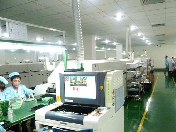
What's the manufacturing process of SMT assembly?
A PCBA order starts with a range of preparation procedures. Processing and handling teams analyze the customer’s data and prepare internal design data for PCBA production, to resolve all questions and details with the customers.
Components Sourcing
Electronic components pass through the incoming control at the warehouse for quality and quantity. The components are kept in the electrostatic discharge area within a controlled environment. Components that require special conditions are stored in dry storage cabinets. In accordance with the production schedule, components are transferred to the
PCBA sites, where they are installed in feeders. Prior to starting the order, PCBs for automatic SMT assembly can be arranged in panels for assembly convenience and optimization. These panels have fiducial marks and process keep out zones or fields for smooth transportation. Along the entire automatic assembly line each board is labeled with an individual code to track the product through all stages of production and quality control. All product data is integrated into a cohesive manufacturing management system.
PCB Fabrication and Stencil
In accordance with the smart manufacturing concept, screen printing is the main method of applying solder paste to printed circuit boards in mass and medium scale production. Stencils are made from high quality stainless steel by the method of laser cutting. The stencil apertures are designed to follow the pattern and location of the pads on the PCB. The bare board will be fabricated following up the buyer’s requirements and instructions in GERBER file and BOM file. Before the actual production, we will have to make agreements about PCB base material, surface finish, solder mask, silkscreen, etc.
Solder Paste
It is important to obtain the right apertures and stencil thickness to ensure the correct volume of solder Paste, which is applied to achieve the desired quality of the soldered joint. Solder paste is a powdered solder alloy combined with a flux plus some minor additives. The flux formula helps to protect the contact surfaces from oxidation and has tacky properties that ensure components stay in position until soldering. Solder paste is applied onto the surface of the pads by automatic screen printers. The printers are equipped with a machine vision system, which ensures the precise alignment of the stencil with the board. The paste is pressed with a special squeegee through the apertures of the stencil onto the contact pads of the PCB. The quality of the application of soldering paste is controlled by a 3d optical inspection machine, which evaluates the volume and accuracy of the solder paste application, deposits on the PCB contact pads as well as other possible defects.
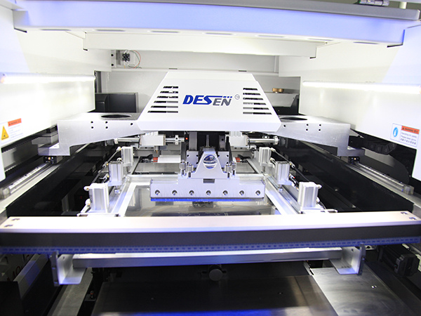
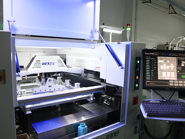
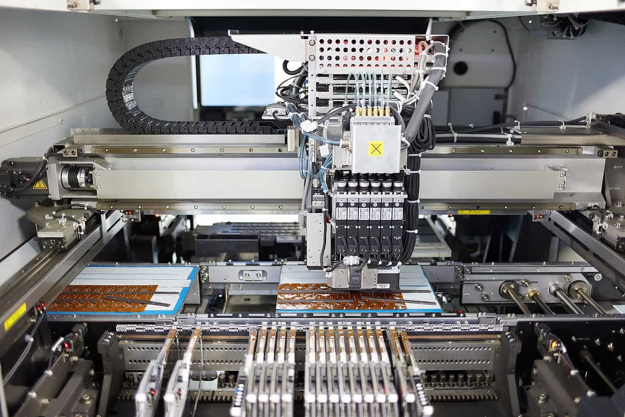
SMD Placement
SMD placement machines arrange components on the PCB in accordance with the design documentation using a pre-written program. Before the assembly process starts, the machine’s camera determines the coordinates of the reference marks on the panel for correct positioning on the PCB‘s.
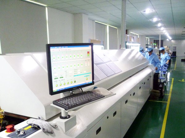
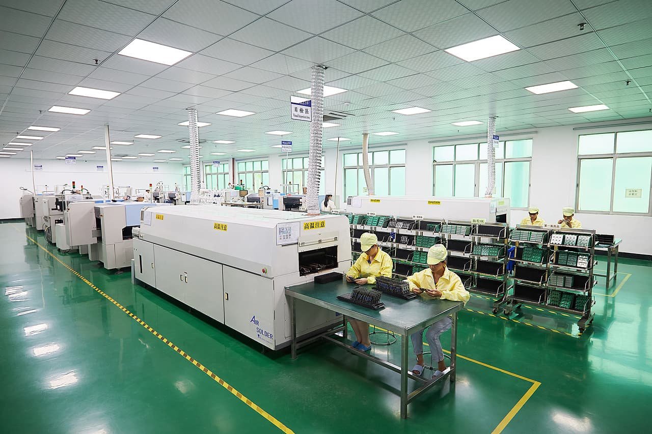
Reflow Soldering
The printed circuit board with installed components moves along the conveyor to the convection reflow solder oven. These state-of-the-art reflow ovens have from 6 to 14 zones each with a different temperature control for uniform and smooth heating and cooling of the PCB. All ovens are able to provide soldering both with leaded and lead-free technologies. The automatic optical inspection system controls the product quality.
PCB Inspection
After soldering, the machines are able to control many parameters. The absence of components deviations in component positioning, the polarity, the bridging between leads, the coplanarity and other parameters and also evaluates the quality of soldered connections, the height and width of the solder fillet as well as compliance with local and IPC standards. The boards on which defects were detected are sorted into a separate magazine of the automatic loader and passed on to the operator. When scanning the PCB‘s barcode, the inspection results are displayed on the screen. The controller evaluates the quality of the soldered connections and if defects are detected the board is passed on to a reworking station statistical process control. SPC is a tool for managing the product’s quality immediately in the production process.
THT Assembly
After the SMD components assembly, the THT components are installed and selectively soldered automatically compared with classic wave soldering. In this technology not all of the underside of the board with components comes into contact with the solder but certain parts of the PCB. Individually one at a time those that are directly subject to soldering. This method allows for the high-quality assembly of complex double-sided boards with high component density. A drop jet fluxing device moves under the lower surface of the PCB and applies the flux only where necessary. Soldering takes place in an inert nitrogen environment which significantly improves the quality of the process. Finished electronic modules pass through the final quality control stage. The operator performs visual quality control of each module using state-of-the-art inspection equipment, including stereo microscopes. The finished modules are packed into a protective anti-static film and sent to the customer.
SMT Assembly Data Acquisition
Quality data is collected and analyzed by a special consolidated software that helps process engineers to improve the current process. The system stores and analyzes the most detailed product characteristics including images, 3d models and measurement results. The link function allows for comparing data from the SPI and AOI systems to conduct parallel analysis. This makes it possible to identify and eliminate the causes of defects. The quality of soldered components with bottom terminated components cannot be determined with optical systems boards. These components are checked at the x-ray inspection machine. An x-ray allows us to control the standard parameters of soldering quality, evaluate the number of voids, check the integrity of the internal PCB conductors and components and if necessary, get high quality images.
What Are The Difference between SMD and SMT?
There are many advantages of the SMT over the THT. Some of the advantages are discussed on the right:
SMT Technology
VS
SMD Technology
The difference between these acronyms SMD and SMT and what they actually mean so you might have heard of SMD LEDs or whatever this just means surface mount and we have two acronyms one of them is SMT that stands for a surface mount technology. SMT is a whole idea that you’re able to mount components on the top of the surface of the PCB. PCB being the printed circuit board and we have an explainer for that one already actually you see how on the back of some board there’s some foam tape but what you don’t see are any components or any little legs of components sticking through compared with this other one in the image given below.
There’s holes in the original PCB and we’ve stuck components through and soldered them on with a soldering iron by contrast the surface mount technology on this circuit everything is mounted on the surface so SMT stands for surface mounted technology and SMD stands for as a surface mount devices so things like LEDs, transistors, resistors and things like that a lot of these come in packages that sit on top of the surface of the LED and instead of soldering them with a soldering iron and sticking them through the board instead you solder on top.